Revisiting my Optical Communications Receiver Project from 2021
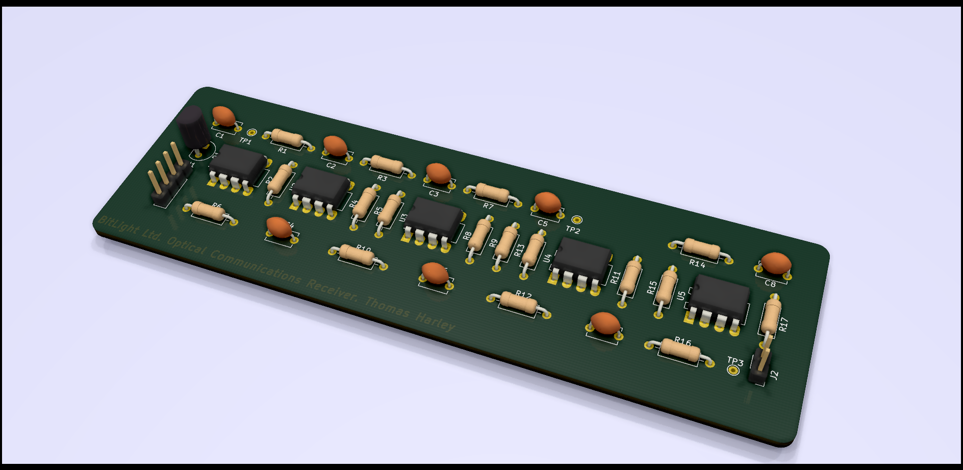
In the third year of my university degree I designed and implemented an analog optical communications receiver for one of my courses. In this post I want to revisit that design and the final report I wrote for the course. I want to explain the design process, how and why I made the decisions I did and cover the simulation steps to verify performance and the final implementation using KiCad.
1 Introduction
The objective of this project was to develop a design that is ‘suitable for traditional optical fibre communications’ as well as ‘visible light communications (VLC/LiFi)’ 1. The following is a very high level overview of the optical receiver circuit. The first stage of the design is a photo-diode used to convert light signals to an electrical current. A trans-impedance amplifier (TIA) is then used to amplify and convert this current signal into a voltage and a high pass filter (HPF) removes any potential DC offset that may develop.
A Low Pass Filter stage (LPF-1) is used to restrict the bandwidth of the transmitted signal in order to reduce noise and remove unwanted signal components. The first amplifier stage (AMP-1) is used to increase our signal amplitude in preparation for our post-amp. A second Low Pass Filter (LPF-2) performs further signal attenuation and finally a Post-Amplifier (AMP-2) performs a large amplification of the voltage signal to achieve our desired peak to peak measurement.
2 Design Process and Justification
Trans-Impedance Amplifier (TIA)
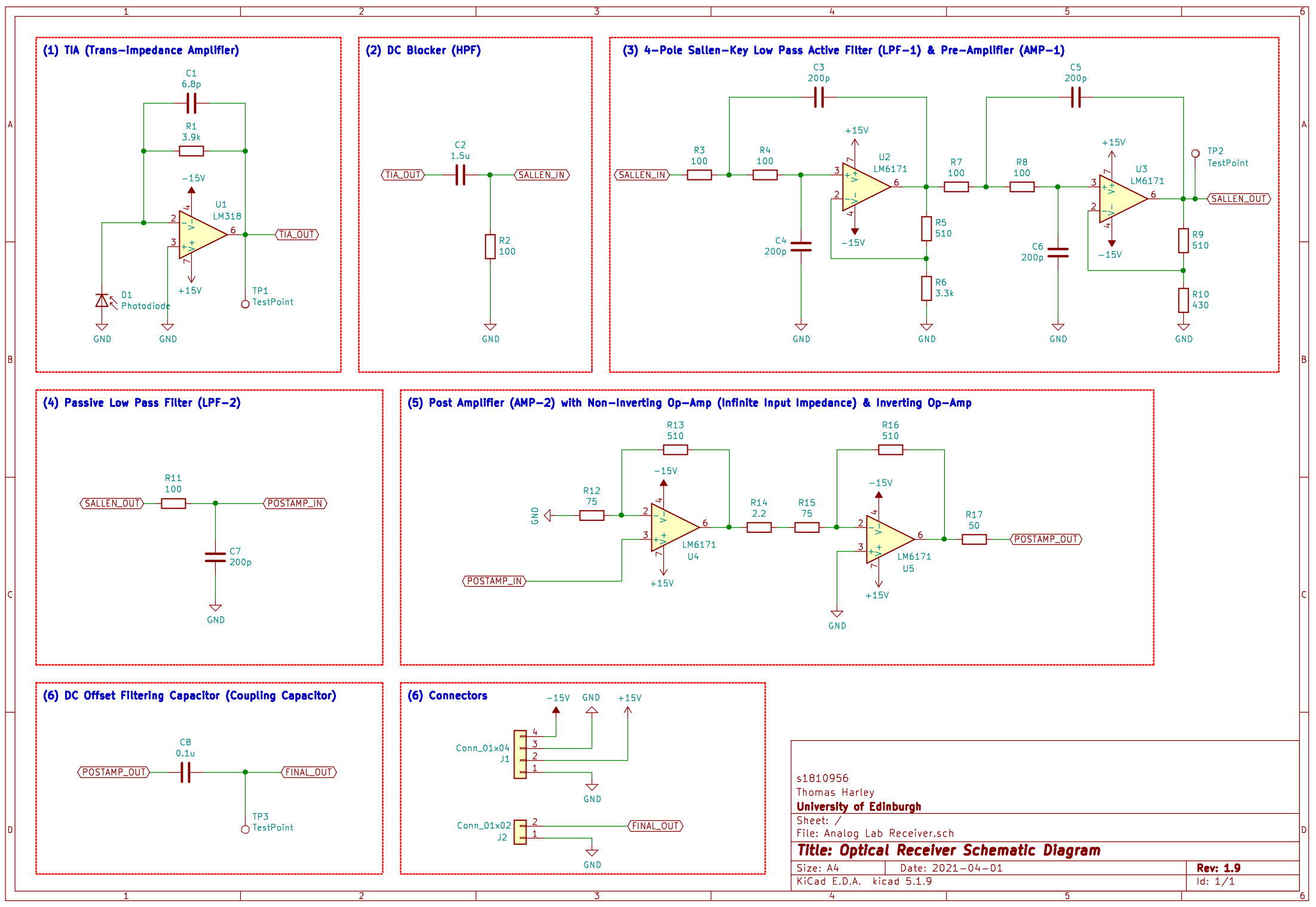
The schematic diagram below shows the fully completed circuit design. Any numerical references made to components throughout the report will be taken from this schematic. The TIA consists of an inverted op-amp configuration. The feedback resistor $R_1$ amplifies the current signal from the photodiode into a voltage signal. The feedback capacitor $C_1$ is utilised to improve stability. We must choose values for $R_1$ and $C_1$ and we must choose an op-amp. Our output voltage $V_{out}$ is given by:
\begin{equation} V_{out} = -I_{pd}R_1. \end{equation}
where $I_{pd}$ is our photodiode current. We may therefore assume that in order to achieve optimum gain at this stage we want to set $R_1$ to be a high value. However, the higher the value of $R_1$ the greater the risk of instability in the frequency response. The design specification of the TIA is that we achieve a 3db bandwidth ($f_c$) of between 5 and 8MHz so our response must be very stable 1. This means we want to set a moderate value of $R_1$ at the cost of a potentially higher gain. The bandwidth $f_c$ is given by:
\begin{equation} f_c = \sqrt{\frac{GBW}{2\pi R_1C_t}} \end{equation}
where $GBW$ is the gain bandwidth product of the op-amp and $C_t$ is the total input capacitance given by: $C_t = C_{pd} + C_{in} = 2pF + 10pF = 12pF$. Where $C_{pd}$ is the built in capacitance of the photodiode and $C_{in}$ is the input capacitance of the op-amp.
According to equation 2 above, picking an op-amp with a high $GBW$ will require a higher $R_1$ value to achieve the specified 3db bandwidth ($f_c$) of between 5 and 8MHz. Therefore we opt for the LM318 with a $GBW$ of approximately 18MHz over the LM6171 which has a $GBW$ of 100MHz 2 3. This allows us to keep $R_1$ low and not introduce further instability. It also has a lower cost and a moderately good slew rate of $50V/\mu s$. We want to aim for an $f_c$ value near the top of the 5-8MHz range. This is because we will be cascading multiple frequency response stages in the receiver resulting in a lower overall $f_c$ 4. By picking a value of $3.9k\Omega$ for $R_1$ we calculate the following:
\begin{equation} f_c = \sqrt{\frac{GBW}{2\pi R_1C_t}} = \sqrt{\frac{(18\times10^6)}{2\pi (3900)(12\times10^{-12})}} = 7.823MHz \end{equation}
This meets our specification and is near the top of the range. Finally, even though by picking a moderate value for $R_1$ we have hopefully reduced instability it is still a good idea to include a feedback capacitor $C_1$. The optimum value for $C_1$ is given by:
\begin{equation} C_1 = \sqrt{\frac{C_t}{2\pi R_1(GBW)}} = \sqrt{\frac{(12\times10^{12})}{2\pi (3900)(18)}} = 5.2pF. \end{equation}
This exposes another strength of choosing the LM318 over the LM6171. The lower $GBW$ means our capacitor will be larger and easier to source. Simulating these preliminary design choices in LTSpice we find the 3db bandwidth to be higher than expected. This is likely due to natural differences between the estimated theoretical equation values and practical values. By increasing our feedback capacitor to $6.8pF$ we bring our $f_c$ down to approximately 7.12MHz which is much closer to our expected value. Now we have our final design values we can calculate our expected $V_{out}$ using equation 1. Our $I_{pd}$ peak amplitude is given in the specification as $1\mu A$ so:
\begin{equation} V_{out} = -I_{pd} \times R_1 = -(1\mu A)(3900) = -3.9 \times 10^{-3}V \end{equation}
Since this is only our amplitude we get a peak to peak voltage magnitude of $7.8mV$ Simulating in LTSpice gives a very similar value of $7.75mV$.
DC Blocker/ Passive High Pass Filter (HPF)
The High Pass Filter consists of a capacitor $C_2$ and a resistor $R_2$ (as shown in the schematic diagram). In this arrangement the capacitor has a very high impedance at low frequencies. This means the HPF blocks DC and also attenuates low frequency signals that are undesirable. The design specification of the HPF requires a 3db cut-off frequency ($f_c$) of $<2kHz$ 1. $f_c$ is given by the following expression:
\begin{equation} f_c = \frac{1}{2\pi R_2C_2} \end{equation}
Through calculations using equation 6 it is found that suitable values for $R_2$ and $C_2$ are $100\Omega$ and $1.5\mu F$ respectfully. Plugging those numbers into the formula we get:
\begin{equation} f_c = \frac{1}{2\pi R_2C_2} = \frac{1}{2\pi (100)(1.5\times10^{-6})} = 1.066kHz \end{equation}
This is within range. Performing a frequency response AC simulation in LTSpice shows a 3db cut-off frequency of almost exactly $1.066kHz$ which shows our circuit performance matches our theoretical calculations. Connecting to our TIA we measure that the DC offset has been reduced to just $-102.28\mu V$. The last thing to verify is that there is no loading between stages. The $V_{out}$ of our TIA has not dropped so no loading has occurred.
4-Pole Sallen-Key Low Pass Active Filter (LPF-1)/ Pre-Amplifier (AMP-1)
The schematic diagram above shows that this stage consists of 2 2-Pole Sallen-Key configurations cascaded together in order to meet the design requirement of a fourth order LPF-1 1. The advantage of a Sallen-Key design is that we can incorporate our LPF-1 and AMP-1 stages together. Examining the first sallen key stage, and again using references from the schematic diagram, we need to set values for $C_3$, $C_4$, $R_3$, $R_4$, $R_5$, $R_6$ and choose our op-amp. We also need to consider our Q factor and choose a filter type.
Starting with frequency response, according to our specification we want to achieve a 3db cut-off frequency ($f_c$) of $5-8$MHz 1. Again we will aim for the high end of the range. From a Texas Instruments report on Low Pass Filter Design 5 we know that:
\begin{equation} FSF \times f_c = \frac{1}{2\pi \sqrt{C_3C_4R_3R_4}} \end{equation}
where $FSF$ is frequency scaling factor. Frequency scaling factor depends on the type of filter we design. We are going to be designing a ‘Butterworth’ filter as they give the ‘maximal flat response’ 5 which is a key specification of our design in the lab manual 1. For Butterworth, the FSF is 1 which makes our calculations easier. We can further simplify equation 8 by making $C_3 = C_4$ and $R_3 = R_4$. We are left with:
\begin{equation} f_c = \frac{1}{2\pi R_3C_3} \end{equation}
Simplifying the mathematical expression in this way comes with the disadvantage of reduced control over our circuit output. We now choose our resistor and capacitor values. As was said previously we want an $f_c$ at the higher end of the range. We also want a relatively high capacitor value, above $100pF$ 6 so that the $C_{in}$ of our op-amp or any other stray capacitance does not dominate. Considering all these factors values of $200pF$ ($C_3, C_4$) and $100\Omega$ ($R_3, R_4$) were selected. Plugging into the formula we get:
\begin{equation} f_c = \frac{1}{2\pi R_3C_3} = 7.95MHz. \end{equation}
Now we consider the amplification part of the Sallen-Key. First, we select our op-amp. We want to achieve a high bandwidth with this design and also achieve a moderate gain. Examining the following approximate expression:
\begin{equation} GBW = gain \times f_c \end{equation}
It is clear that in order to not accidentally restrict our 3db bandwidth ($f_c$) we require a high $GBW$. This makes the LM6171 ideal with its 100MHz $GBW$ 3. The amplification circuit is a non-inverting amplifier configuration so our gain is given by $1 + \frac{R5}{R6}$. For the LM6171 the ideal feedback resistor for best performance is $510\Omega $ 3 so we will set $R_5$ to that. Now we have to determine $R_6$ by considering our desired Q factor. For a 2 stage (4-pole) Butterworth Sallen-Key design the Q factor of the first stage should be $0.5412$ 5. Because we set $R_3 = R_4$ and $C_3 = C_4$ our Q factor is given by the simplified expression:
\begin{equation} Q = \frac{1}{2-K} \end{equation}
where $K = 1 + \frac{R_5}{R_6}$. So combining the two expressions and subbing in $510\Omega $ for $R_5$ and $0.5412$ for Q, we determine the $R_6$ value to achieve best Q factor is $3.35k\Omega$. The closest common value is $3.3k\Omega$.
We design the second stage of the Sallen-Key with the same values in order to achieve the same 3db cut-off frequency ($f_c$). The one alteration we need to make is to our $R_6$ value ($R_{10}$ for the second stage). The desired Q factor for the second stage of a 2 stage Butterworth Sallen Key Filter is $1.3065$ 5 which yields an $R_{10}$ value of $413\Omega$ (using equation 12). The closest common value is $430\Omega$. Note that it is important to place stages with a lower Q factor first to achieve best performance 5. Our overall gain is now:
\begin{equation} G_{sallen} = (1+ \frac{R_5}{R_6})(1+ \frac{R_9}{R_{10}}) = (1+ \frac{510}{3100})(1+ \frac{510}{430}) \simeq 2.52 \end{equation}
This is under the design specification maximum of 4 so is acceptable 1. The expected peak to peak output is given by our $V_{out}$ from the TIA multiplied by this new gain which works out as $\simeq19.68mV$.
Testing the output response of the 4-pole Sallen-Key in isolation in LTSpice we get a cut-off frequency of approximately 7.75MHz which is satisfactory. Combining our Sallen-Key with the HPF and TIA we check for any loading of previous stages.
Passive Low Pass Filter (LPF-2)
The second low pass filter takes the form of a passive filter and is used to further attenuate unwanted signals and reduce noise. It consists of a resistor ($R_{11}$) placed in series with the signal path and a capacitor ($C_7$) in parallel to the next stage (see the schematic diagram). When frequencies are high, the capacitor’s impedance is low relative to the resistor. More voltage is dropped across the resistor and thus high frequency signals don’t pass through the filter. According to the specification we want to achieve an $f_c$ of between 5 and 8 MHz 1. The 3db cut-off frequency is given by the same expression as the HPF:
\begin{equation} f_c = \frac{1}{2\pi R_{11}C_7} \end{equation}
We design the frequency to be the same as our Sallen-Key. Therefore, $R_{11}$ and $C_7$ have values of $100\Omega$ and $200pF$ respectfully. This gives us a calculated $f_c$ of 7.95Mhz. Testing our low pass filter in isolation we find it has a cut-off frequency exactly as expected. Connecting our LPF-2 to the rest of the circuit we test for any loading effects on the previous stage.
Post Amplifier (AMP-2)
The Post Amplifier specification in the lab manual is an amplifier which gives a peak to peak output of $1V$ and has an output impedance of $50\Omega$. It must also remove any DC offset 1. Originally, a design consisting of two inverting op-amps was considered. However, in the early stages of testing it became clear that the input impedance of the first inverting amplifier was not high enough to mitigate a loading effect on the previous stage. This caused an undesirable voltage drop across LPF-2.
In order to mitigate the loading effect a non-inverting op-amp was used for the first stage of the post-amp, taking advantage of the infinite input impedance of the non-inverting configuration 4. This completely eliminated the loading effect on LPF-2. We now have a configuration of one non-inverting and one inverting op-amp. Using reference values from the schematic diagram, the total gain of this stage is given by:
\begin{equation} G_{post-amp} = (1+\frac{R_{13}}{R_{12}})(\frac{R_{16}}{R_{14}+R_{15}}) \end{equation}
Our total required gain to achieve a peak to peak output of $1V$ is given by:
\begin{equation} \frac{1V}{V_{out}} = \frac{1V}{19.68mV} \simeq50.81. \end{equation}
where $V_{out}$ is the output of our Sallen-Key. Knowing all this we can begin to choose our values. The first things to select are our op-amps. From equation 11 we know that in order to have a high gain and not risk lowering our bandwidth we should use an op-amp with a high $GBW$. Therefore we use 2 LM6171 op-amps with $GBW$s of 100MHz 3. We know the optimum feedback resistor to achieve maximum performance of the LM6171 is $510\Omega$ therefore, $R_{13}$ and $R_{16}$ are set to $510\Omega$.
Using equation 15 and the value of our required gain calculated in equation 16 we can now estimate our required values for $R_{12}$ and ($R_{14}+R_{15}$). Once we have our estimates the values are tweaked, using LTSpice simulations, to achieve our exact required peak to peak voltage. The final values are $75\Omega$ for $R_{12}$ and $77.2\Omega$ for ($R_{14}+R_{15}$). $R_{14}$ and $R_{15}$ are split into 2 resistors so common resistor values can be used. This makes sourcing of components for our PCB much easier.
We must now deal with our output impedance requirement. Since we can assume the output impedance of an ideal op-amp is $0$, we simply place a $50\Omega$ resistor ($R_{17}$) at the output of our op-amp.
DC Blocker/ Coupling Capacitor
This final stage is to remove any DC offset at the output of our circuit. A simple coupling capacitor ($C_8$) has been connected in series with the signal path to remove DC. We want to ensure this capacitor passes frequencies over $1.066kHz$ so a value of $0.1\mu F$ works well. Connecting this to our circuit the DC offset becomes negligible ($\simeq-87.46nV$).
3 Design Testing and Performance Analysis
Final Output Waveform Testing and Analysis
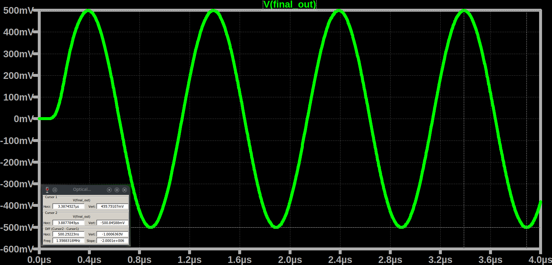
We will be using an LTSpice simulation of our circuit for testing. The LTSpice file used is included with this report. Note that in LTSpice our photodiode is represented by a current source with a capacitor in parallel ($C_{pd} = 2pF$). We perform a transient simulation for $4\mu s$ at $1$MHz for an input current amplitude of $1mA$ (peak to peak input of $2mA$). The waveform shown when we probe the output of our circuit is shown in the figure below.
This waveform is an amplified version of the simulated photodiode current. The LTSpice cursors have been used to accurately calculate the voltage output of our simulation. The final value of our peak to peak $V_{out}$ is $1.0006369V$.
Now we must determine if this output matches our theoretical value. There are three gain stages within the circuit: the TIA, the Sallen-Key and the Post-Amplifier. By combining the gain expressions for the three stages that were derived in Section 2 we can calculate our theoretical output voltage. The expression is as follows:
\begin{equation} V_{out} = I_{pd}R_1(\frac{R_5}{R_6} + 1)(\frac{R_9}{R_{10}} + 1)(\frac{R_{13}}{R_{12}} + 1)(\frac{R_{16}}{R_{14}+R_{15}}). \end{equation}
Plugging in our component values we calculate that $V_{out} = 1.014V$ This is a disrepancy of $\simeq14mV$. This implies that the gain required to achieve a peak to peak voltage output of $1V$ was slightly higher than what our calculations would expect. Therefore, $\simeq14mV$ were lost in the circuit (most likely due to loading between the different stages). Overall, I consider the circuit amplification to be satisfactory. Only a slightly higher gain was required than expected. Such a small voltage drop means the circuit is power efficient. The final measurement taken was the DC offset voltage. Using a cursor on LTSpice and measuring $V_{out}$ at $0\mu s$ gives a measured DC offset of just $-87.46nV$ which meets the criteria of $0V$ as the offset is negligible in comparison to the signal amplitude.
Frequency Response Testing and Analysis
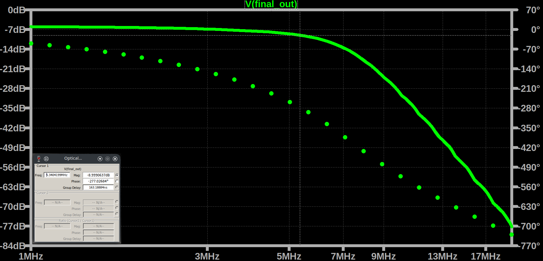
We must now verify that our overall circuit design has a satisfactory frequency response with the correct 3db bandwidth ($f_c$) of between 5 and 8 MHz. We can then compare that figure to our theoretical calculations. A transient simulation was performed as in Section 3. Using step sizes of 500KHz, the frequency was increased from 1MHz to 20MHz. At each stage the peak to peak voltage ($V_{out}$) was measured. Using the following formula:
\begin{equation} G = 20\log(\frac{V_{out}}{V_{out-1MHz}}) \end{equation}
the gain at each frequency was calculated and plotted against frequency in LTSpice to produce a bode plot shown below. The approximate 3db $f_c$ value is labelled by the cursor. You can view the full raw data used to generate this plot in a table below as well.
| Frequency (MHz) | V_out (V) | V_out-1MHz (V) | Gain (dB) |
|---|---|---|---|
| 1 | 1.0006369 | 1.0006369 | 0 |
| 1.5 | 0.98463715 | 1.0006369 | -0.1400059318 |
| 2 | 0.96330264 | 1.0006369 | -0.3302752721 |
| 2.5 | 0.93851477 | 1.0006369 | -0.5567080466 |
| 3 | 0.91020295 | 1.0006369 | -0.8227655074 |
| 3.5 | 0.87750109 | 1.0006369 | -1.14057699 |
| 4 | 0.84191321 | 1.0006369 | -1.500183805 |
| 4.5 | 0.80003556 | 1.0006369 | -1.943344463 |
| 5 | 0.75155544 | 1.0006369 | -2.486309828 |
| 5.5 | 0.69104064 | 1.0006369 | -3.215458504 |
| 6 | 0.61460494 | 1.0006369 | -4.233609349 |
| 6.5 | 0.52373227 | 1.0006369 | -5.623343603 |
| 7 | 0.42429526 | 1.0006369 | -7.45216668 |
| 7.5 | 0.32611005 | 1.0006369 | -9.738246622 |
| 8 | 0.24084963 | 1.0006369 | -12.37061061 |
| 8.5 | 0.17339959 | 1.0006369 | -15.22456896 |
| 9 | 0.12304188 | 1.0006369 | -18.20447112 |
| 9.5 | 0.086899461 | 1.0006369 | -21.22518863 |
| 10 | 0.061469823 | 1.0006369 | -24.23229103 |
| 10.5 | 0.043704565 | 1.0006369 | -27.19499424 |
| 11 | 0.031249485 | 1.0006369 | -30.10867299 |
| 11.5 | 0.022543419 | 1.0006369 | -32.94513462 |
| 12 | 0.016401274 | 1.0006369 | -35.7079786 |
| 12.5 | 0.012009557 | 1.0006369 | -38.41499053 |
| 13 | 0.0088766158 | 1.0006369 | -41.04058182 |
| 13.5 | 0.0066282763 | 1.0006369 | -43.57751821 |
| 14 | 0.0049707071 | 1.0006369 | -46.07716682 |
| 14.5 | 0.0037762453 | 1.0006369 | -48.46432633 |
| 15 | 0.0028736049 | 1.0006369 | -50.83698917 |
| 15.5 | 0.0022002248 | 1.0006369 | -53.15618917 |
| 16 | 0.0017122671 | 1.0006369 | -55.33410004 |
| 16.5 | 0.0013270051 | 1.0006369 | -57.54807844 |
| 17 | 0.0010333033 | 1.0006369 | -59.72097395 |
| 17.5 | 0.00082170698 | 1.0006369 | -61.71119076 |
| 18 | 0.00064684035 | 1.0006369 | -63.78958821 |
| 18.5 | 0.00052277749 | 1.0006369 | -65.6391927 |
| 19 | 0.00041823181 | 1.0006369 | -67.57718905 |
| 19.5 | 0.00033248458 | 1.0006369 | -69.57010012 |
| 20 | 0.00027533564 | 1.0006369 | -71.20828166 |
Frequency Response Data
Inspecting the bode plot above, we can see the 3db cut-off frequency of our overall circuit is $5.3$MHz. This doesn’t seem to match our theoretical calculations as in Section 2 we aimed at each stage to produce a circuit with a 3db cut-off near the higher end of the $5-8$MHz range. However, we must consider the effect cascading multiple stages has on cut-off frequency. We cascade three main frequency response stages together: the TIA, the Sallen Key and our LPF-2. The following formula gives the expected final frequency response 4:
\begin{equation} H_{total}(f) = H_{TIA}(f) \times H_{sallen}(f) \times H_{LPF-2}(f) \end{equation}
We assume for simplicity that each stage was designed with the same cut-off frequency in mind. Therefore, each stages output is 0.707Vin at our 3db cut-off frequency ($f_c$), Using equation 19: $(0.707 \times 0.707 \times 0.707)Vin = 0.353Vin$, where Vin is our peak to peak voltage of $1V$. This means the 3db cut-off frequency ($f_c$) we designed for in each individual stage will lie at approximately $0.353V$ or -9db $(20\log(\frac{0.353}{1}))$. If we inspect our bode plot above we can see that our -9db point lies at $\simeq7.3$MHz which is close to our original theoretical values. Its therefore clear why the overall frequency response has a lower $f_c$. I am therefore satisfied that the performance of this design approximately matches our calculations.
Inspecting the bode plot’s shape we observe a flat passband with no peaking. This is likely due to our choice of a Butterworth filter in the Sallen-Key stage as it gives a ‘maximally flat response’ 5. In terms of our slope in the stop band we see a moderate rate of attenuation. If we wanted a better rate we could change our filter design to a Chebyshev filter. However, that would come at the cost of potential peaking in the pass band 5. Overall I am happy with the frequency response. I think the choice of Butterworth meets the lab manual criteria of ‘maximally flat’ 1, while also giving a good attenuation rate.
Step Response Testing and Analysis
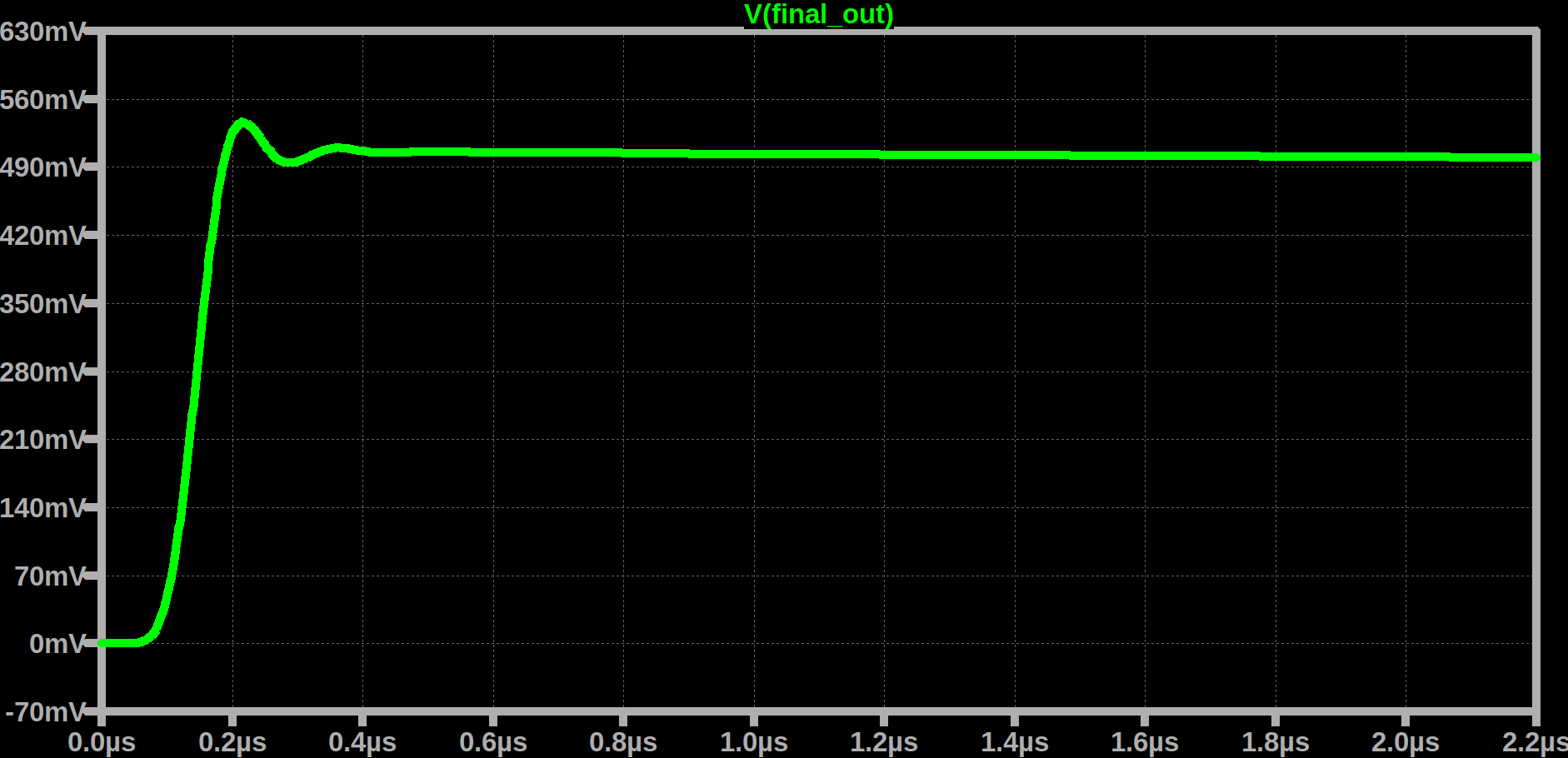
Finally, we must test the design’s Step Response. We set our current source in LTSpice to produce a ‘PULSE’ with a $T_{on}$ of $4\mu s$ and $T_{period}$ of $4\mu s$. We then perform a time domain simulation for $4\mu s$. We get a typical step response curve which settles at a steady state value of around $500mV$ which is what we would expect given our final $V_{out}$. We can perform a number of calculations using information from this simulated response. First to calculate rise time ($t_r$) we find the time it takes to go from $10%$ to $90%$ of our steady state value. In other words the time difference between $50mV$ and $450mV$. This is calculated using our LTSpice cursors and found to be $74.87ns$. Now we can calculate our theoretical bandwidth using the following formula:
\begin{equation} B_{theoretical} = \frac{0.35}{t_r} = \frac{0.3}{74.87\times10^{-9}} = 4.67MHz \end{equation}
This is a difference of $\simeq0.63$MHz when compared to our actual bandwidth found in Section 3. This difference is to be expected as this formula is derived by assuming we are dealing with a simple one stage, one pole RC network 7. Since our circuit is far more complex in nature we cannot expect this estimate to give us an accurate indication of our Bandwidth. Our last piece of analysis is our overshoot percentage. This is calculated from the difference between the peak of our step response and the Y steady state value. Using the following formula we calculate:
\begin{equation} Overshoot_{percentage} = \frac{Y_{peak}-Y_{steadystate}}{Y_{steadystate}}\times100 = \frac{535.96-500}{500}\times100 = 7.192% \end{equation}
We can account for this overshoot by again considering our choice of filter in the Sallen-Key stage. We opted for a Butterworth filter which is expected to give a slight overshoot of this magnitude 8. If we were designing for minimum overshoot we would likely choose a Bessel design as it gives negligible overshoot compared to the Butterworth 8. However, it does not have as flat a response. The LTSpice step response output curve is shown below for further clarification.
4 PCB Layout and Design
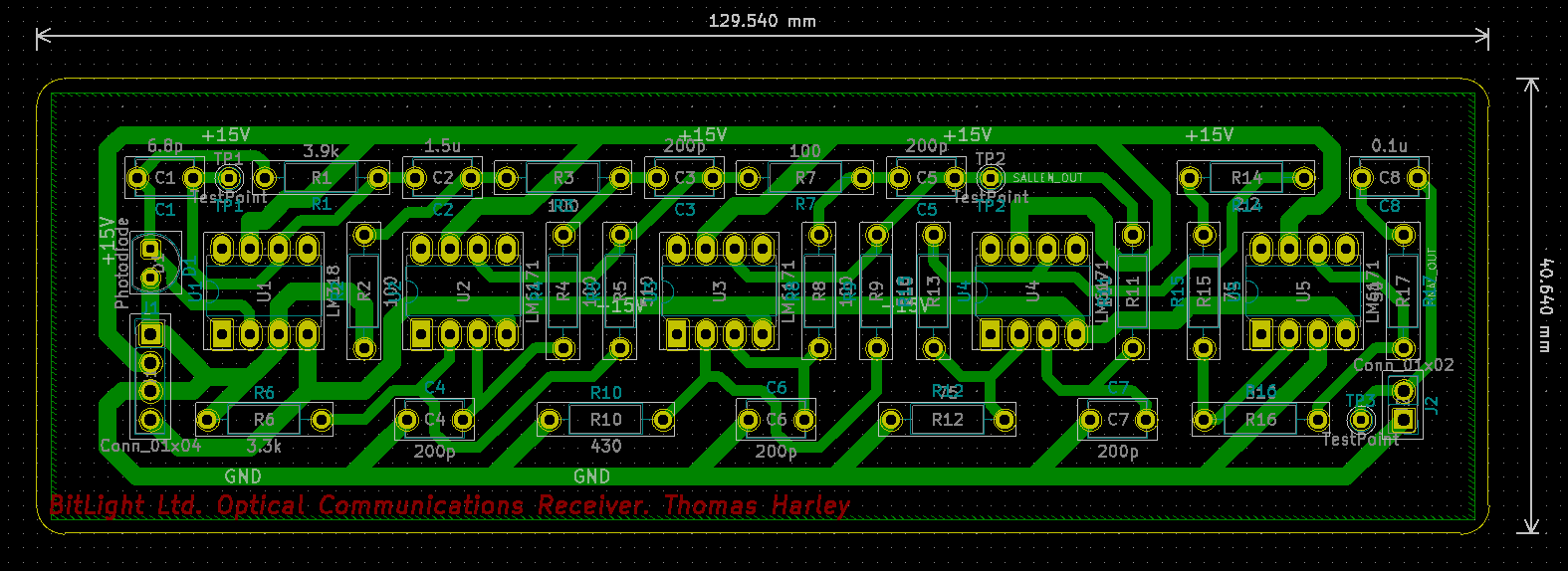
KiCad version 5.1.9 was used to design the PCB board. The project files have been included with this report. Pictures of the PCB layout and 3D Model are shown in the figures below. A four pin vertical connector was used to supply power and a two pin connector was used for our output voltage signal. Widths of $1mm$ were used for signal tracks and $1.6mm$ for power tracks. A minimum spacing of $0.5mm$ is given between tracks on the board. The corners of the PCB have been rounded to reduce sharpness. Test pins have been placed at the outputs of key circuit stages. A gap of $5mm$ has been left between the outermost tracks and the edge of the board due to incomplete photoresist coverage at the edges of the board.

Bill of Materials
A full list of components used for the PCB can be found in the Bill of Materials (BOM) below.
| Description | Part Number | No. | Unit Cost | Total Cost | PCB Ref. |
|---|---|---|---|---|---|
| 6.8pF Cap, THT, 5mm | MC0805N6R8C500A2.54MM | 1 | £0.18 | £0.18 | C1 |
| 1.5uF Cap, THT, 5mm | RHEL81H155K2A2H03B | 1 | £1.00 | £1.00 | C2 |
| 200pF Cap, THT, 5mm | MC0805N201J101A2.54MM | 5 | £0.28 | £1.42 | C3, C4, C5, C6, C7 |
| 0.1uF Cap, THT, 5mm | MPCC50V104KY5U | 1 | £0.17 | £0.17 | C8 |
| Pin Photodiode | 1540051EC3590 | 1 | £0.51 | £0.51 | D1 |
| Conn 01x04, Vert. Pin Header, THT, 2.54mm | 90120-0764 | 1 | £0.94 | £0.94 | J1 |
| Conn 01x02, Vert. Pin Header, THT, 2.54mm | 90120-0122 | 1 | £0.35 | £0.35 | J2 |
| 3.9kΩ Res, THT, 10.16mm | MBA02040C3901FC100 | 1 | £0.15 | £0.15 | R1 |
| 100Ω Res, THT, 10.16mm | MCKNP03WJ0101AA9 | 6 | £0.24 | £1.46 | R2, R3, R4, R7, R8, R11 |
| 510Ω Res, THT, 10.16mm | MBB02070C5100FC100 | 4 | £0.12 | £0.47 | R5, R9, R13, R16 |
| 3.3kΩ Res, THT, 10.16mm | MOR03SJ0332A19 | 1 | £0.14 | £0.14 | R6 |
| 430Ω Res, THT, 10.16mm | MF50 430R | 1 | £0.05 | £0.05 | R10 |
| 75Ω Res, THT, 10.16mm | MCKNP05SJ0750AA9 | 2 | £0.27 | £0.55 | R12, R15 |
| 2.2Ω Res, THT, 10.16mm | MCKNP05SJ022JAA9 | 1 | £0.30 | £0.30 | R14 |
| 50Ω Res, THT, 10.16mm | MCKNP01SJ050KA10 | 1 | £0.08 | £0.08 | R17 |
| LM318 Op-Amp | LM318P | 1 | £1.62 | £1.62 | U1 |
| LM6171 Op-Amp | LM6171BIN/NOPB | 4 | £3.37 | £13.48 | U2, U3, U4, U5 |
| £22.85 |
Bill of Materials (BOM)
-
Dr. Wasiu O Popoola. Analogue Mixed Signal Laboratory 3 Manual. (accessed: 01.04.2021). ↩︎ ↩︎ ↩︎ ↩︎ ↩︎ ↩︎ ↩︎ ↩︎ ↩︎ ↩︎
-
National Semiconductor. LM118/LM218/LM318 Operational Amplifiers. url: http://web.mit.edu/6.301/www/LM118.pdf. (accessed: 01.04.2021). ↩︎
-
Texas Instruments. LM6171HighSpeedLowPowerLowDistortionVoltageFeedbackAmplifier. url: https://www.ti.com/lit/ds/symlink/lm6171.pdf. (accessed: 01.04.2021). ↩︎ ↩︎ ↩︎ ↩︎
-
Dr. Wasiu O Popoola. Loading Effect in Circuit Design. (accessed: 01.04.2021). ↩︎ ↩︎ ↩︎
-
Texas Instruments. Active Low-Pass Filter Design. url: https://www.ti.com/lit/an/sloa049b/sloa049b.pdf. (accessed: 01.04.2021). ↩︎ ↩︎ ↩︎ ↩︎ ↩︎ ↩︎ ↩︎
-
Texas Instruments. Analysis of the Sallen-Key Architecture. url: https://www.ti.com/lit/an/sloa024b/sloa024b.pdf. (accessed: 01.04.2021). ↩︎
-
The Free Encyclopedia Wikipedia. Rise Time. url: https://en.wikipedia.org/wiki/Rise_time. (accessed: 01.04.2021). ↩︎
-
Bonnie C Baker. Howtocompareyourcircuitrequirementstoactive-filterapproximations. url: https://www.ti.com/lit/an/slyt681/slyt681.pdf. (accessed: 01.04.2021) ↩︎ ↩︎
